UV Curing Systems for PCB Manufacturing: Overcoming Challenges and Delivering Precision
In the fast-paced world of printed circuit board (PCB) manufacturing, precision, speed, and reliability are paramount. As electronics continue to evolve toward miniaturization, higher performance, and greater durability, the production processes must adapt accordingly. One critical process in PCB fabrication is UV curing — a technique used to harden or cure photoresist materials, solder masks, conformal coatings, and other UV-reactive substances applied during manufacturing.
While UV curing systems have become indispensable in modern PCB production lines, they also present several challenges that can affect yield, throughput, and overall product quality. This article explores the most common pain points associated with UV curing systems in PCB manufacturing, presents practical and technical solutions, highlights real-world applications, and concludes with insights into how Xinhua Intelligent’s advanced UV curing systems can address these issues effectively.
—

1. Common Pain Points or Challenges
Despite their importance, UV curing systems are not without limitations. The following are some of the most prevalent challenges faced by PCB manufacturers using conventional UV curing setups:
A. Inconsistent Cure Quality
One of the most significant issues is uneven UV exposure across the PCB surface. Variations in lamp intensity, reflector design, or conveyor speed can lead to under-cured or over-cured areas, resulting in poor adhesion, incomplete cross-linking, or thermal damage to sensitive components.
B. Thermal Damage Risk
Traditional mercury vapor lamps emit a broad spectrum of light, including infrared radiation, which generates heat. In high-volume PCB production, this heat can cause warping, delamination, or damage to temperature-sensitive substrates such as flexible PCBs or those with embedded components.
C. Lamp Degradation and Maintenance Costs
Conventional UV lamps degrade over time, requiring frequent replacements and recalibrations. This not only increases operational costs but also leads to unplanned downtime, reducing overall equipment effectiveness (OEE).
D. Environmental and Safety Concerns
Mercury-based lamps pose environmental risks due to hazardous waste disposal requirements. Additionally, operators may be exposed to harmful ozone emissions and UV radiation if proper shielding and ventilation are not in place.
E. Limited Process Control and Flexibility
Many legacy UV curing systems lack precise control over parameters such as wavelength, intensity, and exposure duration. This makes it difficult to optimize the curing process for different materials or complex PCB designs, especially when dealing with multi-layer boards or varying coating thicknesses.

—
2. Practical and Technical Solutions
To overcome these challenges, PCB manufacturers are increasingly turning to advanced UV curing technologies that offer superior control, efficiency, and safety. Below are key solutions addressing each of the above pain points:
A. Uniform Exposure Through LED UV Curing
Light Emitting Diode (LED) UV curing systems provide narrow-spectrum UV output at specific wavelengths (typically 365 nm, 385 nm, or 395 nm), enabling more consistent and targeted curing. Unlike traditional lamps, LEDs do not emit infrared radiation, significantly reducing thermal stress on the PCB. Their directional light emission also ensures even coverage, minimizing shadowing effects.
B. Precise Thermal Management
Modern UV curing systems incorporate intelligent cooling mechanisms and non-thermal light sources (like UV LEDs) to prevent overheating. These systems maintain stable temperatures throughout the curing process, preserving the integrity of delicate substrates and preventing dimensional instability.
C. Longer Lifespan and Reduced Maintenance
UV LED systems have a much longer operational life (up to 20,000 hours or more) compared to mercury lamps (~1,000 hours). They do not suffer from degradation in intensity over time and eliminate the need for frequent bulb changes, thus reducing maintenance costs and increasing system uptime.
D. Eco-Friendly and Safe Operation
UV LED systems are mercury-free, eliminating the environmental hazards associated with lamp disposal. They also produce minimal ozone and operate without generating excessive heat, improving workplace safety and reducing the need for complex ventilation systems.
E. Advanced Process Control and Integration
New-generation UV curing systems come equipped with digital controls, programmable recipes, and real-time monitoring capabilities. These features allow for fine-tuning of intensity, exposure time, and conveyor speed to match the specific requirements of each PCB type. Integration with Industry 4.0 platforms enables remote diagnostics, predictive maintenance, and seamless data exchange with MES/ERP systems.
—
3. Real-World Applications
The adoption of advanced UV curing systems has transformed various aspects of PCB manufacturing. Here are some real-world applications where these systems deliver measurable benefits:
A. Solder Mask Curing
Solder mask application is one of the most common uses of UV curing in PCB fabrication. High-quality UV curing ensures that the mask adheres properly, protects copper traces, and withstands subsequent thermal cycles. With uniform exposure and controlled intensity, UV LED systems ensure optimal cross-linking without damaging underlying layers.
B. Photoresist Development
Photolithography relies heavily on precise UV exposure to define circuit patterns. Advanced UV curing systems enable accurate imaging by ensuring consistent exposure across the entire panel, reducing defects like line width variation and undercutting.
C. Conformal Coating Curing
For PCBs used in harsh environments (e.g., automotive, aerospace, industrial), conformal coatings protect against moisture, dust, and corrosion. UV curing provides rapid and thorough polymerization of these coatings, enhancing protection while maintaining throughput.
D. Flex and Rigid-Flex PCB Manufacturing
Flexible and rigid-flex PCBs require low-temperature processing to avoid substrate deformation. UV LED curing systems are ideal for these applications because they minimize thermal stress and support high-resolution patterning on thin, bendable materials.
E. High-Density Interconnect (HDI) Boards
HDI boards feature microvias and ultra-fine lines that demand exceptional curing accuracy. Precise wavelength control and uniform irradiance provided by modern UV systems ensure reliable curing of dielectric materials and laser-drilled vias.
—

4. Conclusion and Call to Action
As PCB designs become more complex and manufacturing tolerances tighter, the role of UV curing systems in ensuring process reliability and product quality becomes ever more critical. By addressing common challenges such as inconsistent curing, thermal damage, maintenance inefficiencies, and environmental concerns, next-generation UV curing technology offers a robust solution for modern PCB production lines.
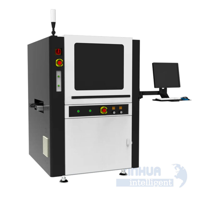
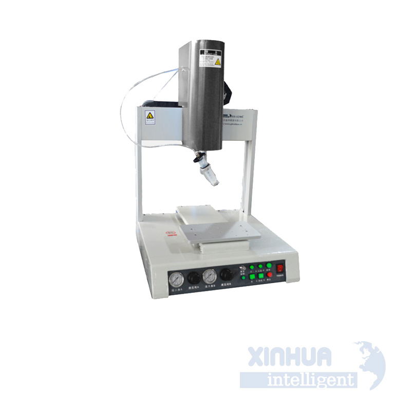
Xinhua Intelligent stands at the forefront of this innovation, offering state-of-the-art UV curing systems tailored for the demands of high-precision PCB manufacturing. Our systems combine advanced LED technology, intelligent process control, and eco-friendly operation to deliver unmatched performance and reliability.
Whether you’re producing standard FR4 boards, flexible circuits, or cutting-edge HDI modules, Xinhua Intelligent’s UV curing solutions are engineered to meet your evolving needs. Contact us today to learn how we can help you enhance your curing process, improve yields, and future-proof your PCB manufacturing operations.
Visit [www.xhuvtech.com](http://www.xhuvtech.com) or contact our team directly to schedule a consultation or request a demo. Let Xinhua Intelligent illuminate the path to smarter, faster, and cleaner PCB curing.
